Key takeaways
X-ray shows the shape, cross-section shows the interface. 2D X-ray images reveal voids, first signs of cracking and their location; metallographic cross-sectioning resolves the interface and shows whether the crack runs along the pad interface, through the solder, or through the substrate. The core of failure analysis is locate first, then dissect — both steps are needed. Concluding from X-ray alone easily leads to a wrong call.
Cracked BGA solder joints are a classic hidden failure: the part looks fine and functions normally, but a crack has already formed inside under thermal cycling or vibration load. Locating it takes a proper analytical method.
1. X-ray: shape and location first
X-ray imaging is the first step. It provides two kinds of information:
Internal joint structure: void fraction inside the solder, ball shape and interface bonding are all clearly visible. An excessive void fraction is an important contributor to cracking.
Preliminary crack location: a wide crack shows up as a linear dark region in the 2D image.
One caveat: conventional X-ray is a two-dimensional projection, so multilayer structures overlap. For QFN and LGA packages, or to view a crack from a specific angle, two-dimensional X-ray with CT or oblique-angle imaging is required.
2. Metallographic cross-section: pinning down the failure interface
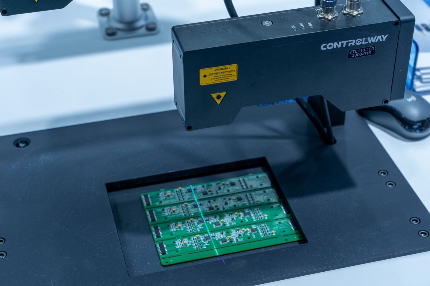
Cross-sectioning means cutting the sample along a planned direction, mounting, polishing and then examining it under a microscope. Its core value is the information X-ray cannot show:
Interface bonding: the most critical information in a cracking failure. It distinguishes whether the crack runs along the pad-to-solder interface, through the solder, or through the PCB substrate.
Intermetallic compound (IMC) thickness: too thin and the interfacial bond is weak, too thick and it cracks through brittleness. Measuring IMC thickness is core data for establishing the root cause.
Kirkendall voids: voids in the IMC nucleate cracks under thermal cycling stress and are a common crack origin.
3. Reading the failure interface
Crack along the pad/solder interface
Common causes: contamination on the pad surface, flux residue, poor wetting between the pad finish and the solder. Corrective direction: improve the PCB pad process and optimise the soldering profile.
Crack through the solder
Common causes: solder composition mismatched to the process, cooling rate too fast, stress concentration at internal voids. Corrective direction: adjust the soldering profile and optimise the solder paste characteristics.
Crack at Kirkendall voids
Common cause: excessive high-temperature ageing time or temperature making the IMC too thick. Corrective direction: control the reflow peak temperature and the time above liquidus, with tighter limits for silver-bearing pastes.
4. The complete analysis sequence
- Step 1 — verify the failure: confirm the failure symptom and record the conditions (number of thermal cycles, vibration level, state at the moment of failure)
- Step 2 — visual and X-ray: rule out obvious external damage, observe the internal shape
- Step 3 — targeted cross-section: cut at the location the X-ray indicates and examine the interface closely
- Step 4 — composition analysis: run EDS on the failure interface to confirm elemental diffusion and compositional anomalies
- Step 5 — root cause: combine the failure conditions, interface morphology and process information into one judgement
- Step 6 — verification: run a confirmation test with the optimised process to prove the corrective action works
5. Advice for designers
The root cause of a solder joint crack is often planted at the design stage: a PCB layout that ignores thermal stress distribution, devices placed too close to the board edge, large thermal pads without stress-concentration design. The value of failure analysis is not only locating the failure but feeding the root cause back to design, closing the loop.